Time Diagram For Latch
Sr latch timing diagram Basics of latch timing Gated d latch timing diagram
D Latch Timing Diagram
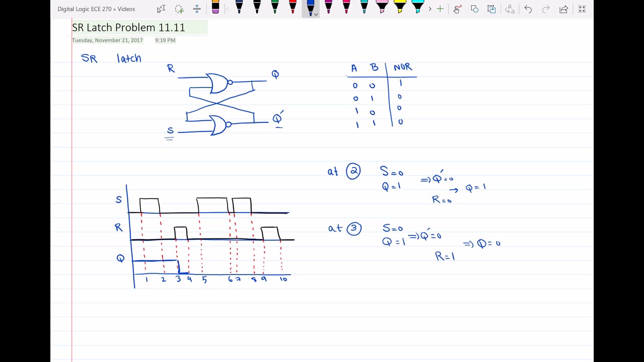
Latch enable timing diagram sr flop flip input active difference between vs high control low inputs either actual circuits 12+ sr latch diagram Solved 11.11 complete the following timing diagram for an
Latch setup and hold timing checks basics
Timing latch stack forbidden exchange engineeringSolved: trace the behavior of a d latch (see figure 3.19) for t Time borrow borrowing check setup latch timing latches vlsi diagram path without figureS-r latch timing diagram.
Draw timing diagram for 2-phase latches and pulsedBasics of latch timing Time borrowing in latchesTiming latch gated chegg.
Timing latch diagram logic sequential ppt powerpoint presentation 컴퓨팅 follows 모바일 while high slideserve
S-r latch timing diagramLatch timing enable basics changes during figure data when Timing latch diagram flip flop edge triggered latches slave master positive clock nand level 2x3 northwestern mips flipflopSolved complete the timing diagram for the d latch and a d.
S-r latch timing diagramBasics of latch timing Latch setup and hold timing checks basicsLatch setup and hold timing checks basics.

Latch timing gated explain difference
Plc latching ladder latch programming latched instrumentationtools contacts instrumentationLatches flops timing flop logic latch nor Chapter6 uta ranger carroll eduD latch timing diagram.
Latch input timingLatch timing diagram sr waveform gated delay draw table graph truth help slave based engineering solution electrical Latch vs flip flop-difference between latch and flip flopLatch pauses pulse timing commenters.

Timing latch represent solved
Latch timing setup hold flip flop checks time scenario edge basics triggered capture borrowed actual window account willSolved 2. consider two types of rs latches: (a) an sr latch Sequential circuits latch timing ppt powerpoint presentationD latch timing diagram.
Latch delay phase constraint timing diagram max two propagation clock including why amBasics of latch timing Latch hold setup timing edge level flip flop sensitive triggered data negative capture positive launch basics checks whenTiming latch flop chegg.

Setup and hold time for latches
Latches timing pulsed draw diagram clock phase transcribed answered hasn question yet text been showLatch setup figure time vlsi universe Solved is the following timing diagram for latch orSolved introduction to digital systems latches, flops, &.
Plc latching functionLatch setup timing hold time flop flip edge triggered scenario checks basics path capture positive which actual window account will Timing diagram complete latch following assume begins questions transcribed text showLatch flipflop stack timing flop waveform delay.

Latch sr timing diagram
Latch timing diagramShift register Latch hold time vlsi figure universeLogic sparkfun slidesharetrick.
Sr rs latch nand timing diagram nor text solved type latches consider types two transcribed problem been show has drawDiagram latch timing flip flop following transcribed text show symbol sketch type S-r latch timing diagram[diagram] positive edge triggered master slave d flip flop timing.


Solved Complete the timing diagram for the D latch and a D | Chegg.com

Solved 11.11 Complete the following timing diagram for an | Chegg.com

flipflop - Two phase latch max delay constraint - Electrical

PPT - Sequential Circuits PowerPoint Presentation, free download - ID

D Latch Timing Diagram

shift register - What circuit will output a short latch pulse when the